Facilities & Labs
For more than 40 years, the research groups at the PlasmaCheM Hub have served as a national and international leaders in plasma science and technology applied to the development of multifunctional materials by advancing the study of innovative chemical and plasma processes for the synthesis, surface functionalization and engineering of materials, nanostructures and devices.
The research activities are focused on the following 4 strategic objectives:
Facilities available @ PlasmaCheM include:
- 4 labs for materials growth and processing also by plasma-assisted processes: Graphene and 2D Materials Lab, Chemical Vapor Deposition (CVD) Lab, Plasma Technologies Lab and Laser-Plasma Lab.
- 1 Bio Lab including facilities for the manipulation of cellular interactions with biomaterials
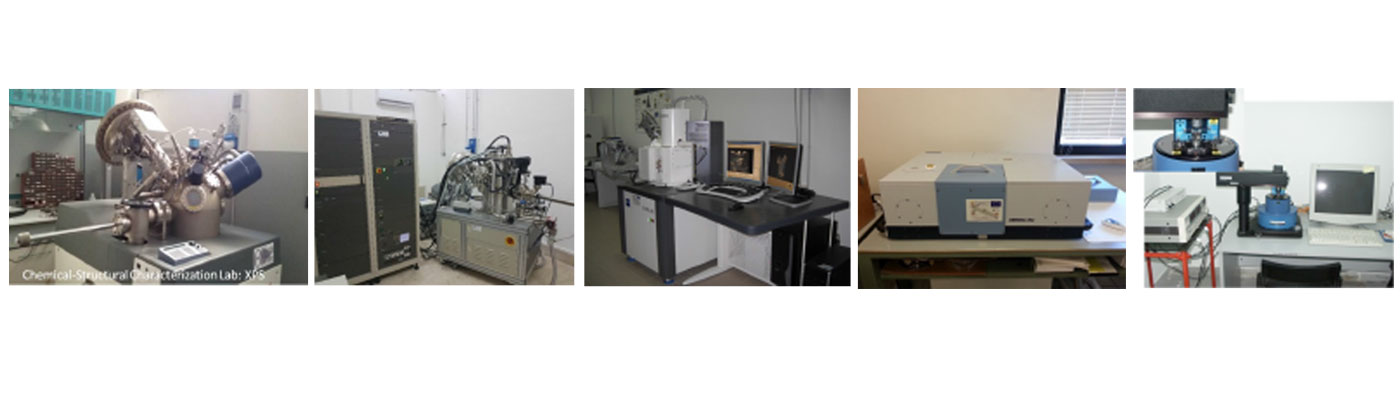
- Labs for advanced characterizations Chemical-Structural, Optical and Electrical characterizations.
- An ancillary lab is dedicated to wet chemistry.
- Extensive microscopy and spectroscopy facilities are also available for SEM, XPS, Raman, AFM, chemical characterization, and others.
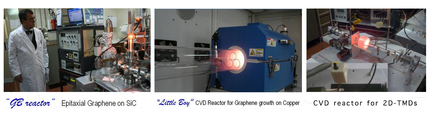
This lab, also known as Apulian Graphene Lab, is specialized in the production of high quality graphene layers by CVD (Chemical Vapor Deposition) and Epitaxy on SiC (silicon carbide), and in reliable plasma-chemical methods designed for surface functionalization of graphene (fluorination, hydrogenation, oxidations). Also, the CVD synthesis of 2D-TMD (WS2, MoS2) is investigated.
The lab is equipped with three reactors:
- Little Boy (CVD graphene on large area 10cmx10cm);
- GB-Reactor (epi-growth of graphene by SiC);
- Big Boy (CVD growth of TMD).
Following that, the materials are characterized and investigated at the nanoscale, ultimately to be used for a variety of specific application spanning from photonics, photovoltaics and for sensors.
Responsibles: Maria Losurdo, Giuseppe Valerio Bianco
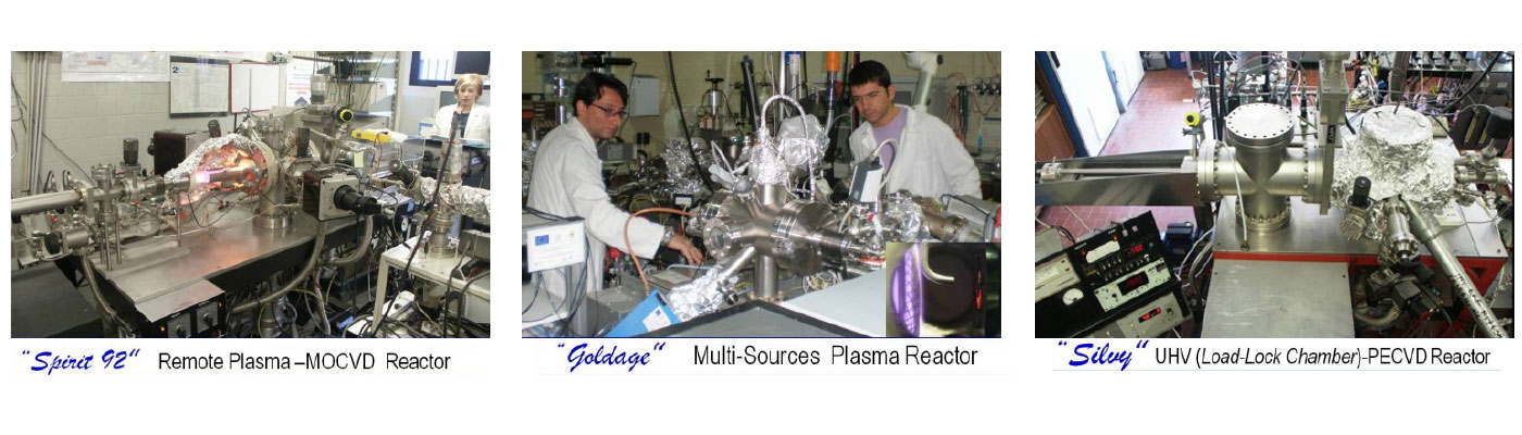
The CVD lab includes:
- Remote plasma MOCVD system (Spirit 92 reactor) designed for the growth and processing of III-V semiconductors (InP, GaN, InN,…);
- CVD-sputtering assisted system (Goldage) for the growth of oxides, TCOs, ceramics, and metals;
- PECVD system (Silvy reactor) for the growth of Si and SiGe based alloys. All our system have a plasma integrated source as well as in-situ real-time monitoring techniques of spectroscopic ellipsometry, mass spectrometry and optical emission spectroscopy for the kinetic analysis of growth and monitoring of processes and material quality.
Following that, the materials are characterized and investigated at the nanoscale, ultimately to be used for a variety of specific application spanning from photonics, photovoltaics and for sensors.
Responsible: Maria Losurdo
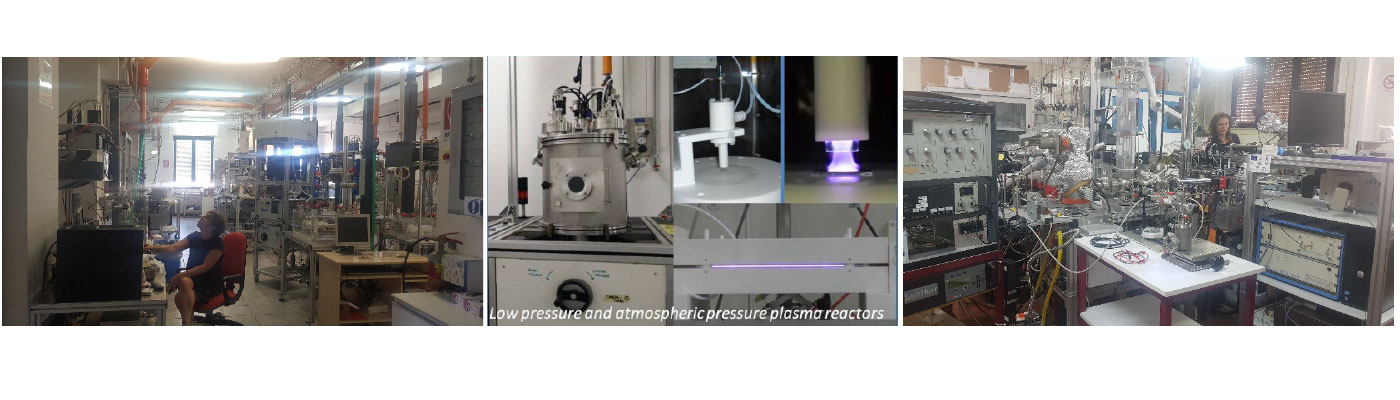
LOW PRESSURE PLASMA
- PLASMA TUBE and PLASMA TROLL with interbal or external moving electrodes;
- FLUOMEM home made PECVD reactor. Low pressure equipment with magnetron sputtering for codeposition processes or multilayer coatings;
- NANOS Reactive ion etching home made plasma reactor;
- SPACE-SHIP mounting 3 independent movable 2” magnetron sputtering sources.
ATMOSPHERIC PRESSURE PLASMA
- Petri-Plas+ Volume-DBD designed by INP-Greifswald, Germany;
- DBD reactors equipped with pneumatic aerosol generators for nanocomposite coatings deposition;
- Plasma Jet with coaxial cylindrical DBD electrode configuration.
Responsibles: Maria Losurdo, Fabio Palumbo
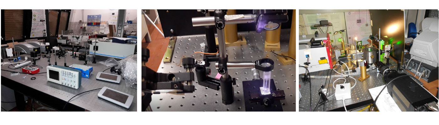
The laser plasma lab si mainly devoted to laser induced plasma diagnostic and to the production of nanoparticles, nanostructures and thin film by laser ablation. The tecniques are: Laser Induced Breakdown Spectroscopy (LIBS), Nanoparticle enhanced LIBS (NELIBS), Pulsed Laser Ablation in Liquids (PLAL), Pulsed laser deposition (PLD).
The instrumentations consists of:
- Five Nd:YAG laser sources, with SHG and THG.
- Three pulse generators for synchronization of lasers with acquisition system.
- Optical bench for bending optics.
- Detection system made of two monochromators and two ICCD.
- Different set of optics for different experiments (LIBS, NELIBS, LIF, Stimulated Raman Scattering, spectroscopy during PLAL and PLD).
- Reaction chamber equipped with different viewport for spectroscopy with vacuum pump.
- High pressure liquid chamber with HPLC pump equipped with different viewport for spectroscopy (LIBS, PLAL).
- Oscilloscopes.
- ICCD for imaging.
- High speed camera for shadowgraph measurements.
- Absorption Spectrometer.
- Chemical glassbench and pH meter.
Responsible: Marcella Dell’Aglio
- Heracell CO2 incubator for growing eukaryotic cell lines.
- Herasafe biological hood to manipulate eukaryotic cell lines.
- Centrifuges to collect cells/RNA/cDNA.
- Mixing shakers orbital.
- Autoclave.
- Biorad Power supply and electrophoresis sistem to analyze DNA/proteins for studying gene expression.
- Applied Biosystems® Veriti® 96-Well Thermal Cycler to amplify cDNA fragments to study specific gene expression of cells grown on different surfaces (PCR).

Responsibles: Roberto Gristina, Eloisa Sardella
- Several scanning probe microscopes with various measurements modes such as atomic force microscopy (AFM), lateral force microscopy (LFM), electrical force microscopy (EFM), magnetic force microscopy (MFM).
- Zeiss Supra 40 Field-Emission Scanning Electron Microscope.
- THETAPROBE THERMO X-ray Photoectron Spectrometer.
- Bruker VERTEX 70v FTIR spectrometer.
- Fluorescence (Zeiss Axiomat) and inverted (Nikon Eclipse) optical microscopes.
- ALPHA-STEP D-120, Tencor Instruments for 2D profiling.
- KSV CAM200 measuring surface and interfacial tension, static and dynamic contact angles.
Responsibles: Fabio Palumbo, Fiorenza Fanelli
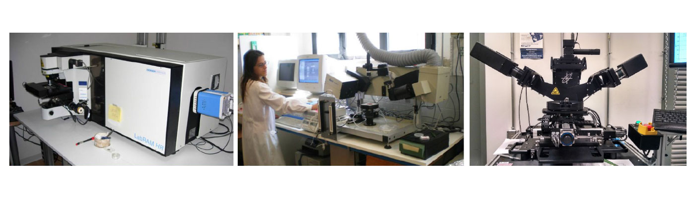
The optical characterization lab includes:
- 4 different spectroscopic ellipsometers covering the UV-VIS—NIR spectra range also equipped with temperature programmable cells for the analysis in liquids and controlled gas atmospheres;
- a high resolution Raman spectrometer equipped with 4 lasers and a temperature programmable sample stage;
- various visible and FTIR spectrofotometers;
- several optical microscopes;
- photoluminescence and fluorescence spectroscopies.
Responsibles: Maria Losurdo, Maria Michela Giangregorio
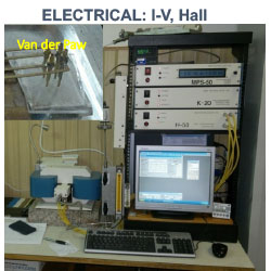
Our expertise is on the (current-voltage) I-V characterization of semiconductors and related materials as well of photovoltaic solar cells. The facilities available in this lab are: Van-der Pauw/Hall instrument to measure the resistivity and the Hall coefficient (MMR) also as a function of temperature; instrument for the spectral responsivity of the photocurrent; high resistance electrometer (Keithley) for sensitive measurements on thin films and 2D material; metal evaporator (Balzers) for electrical contacts, (metals currently being used include Au, Ag, Al, In) with monitored and controlled thickness by quartz microbalance; high vacuum chamber with high temperature heater for electrical measurements under controlled gas environment.
Responsibles: Maria Losurdo, Giuseppe Valerio Bianco
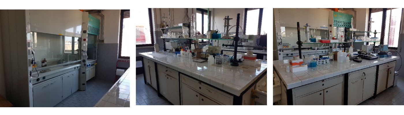
Applications:
- Chemical etching.
- Chemical cleaning of semiconductors wafers.
- Surface functionalizations (thiols, silazanes,amines, amides, siloxanes,etc..).
- Deposition of nanoparticles from colloidal solutions.
- Drop casting of organic films.
- Self-assembled layers of biomolecules, proteins, DNA.
Equipment:
- Solvent cup drain.
- Ultrasonic bath.
- Temperature controlled hotplates.
- Dual process timers.
- Controlled N2 atmosphere operation.
- Bruwer CEE200 High Precision Spin coater.
- QCM-D Q-SENSE quartz crystal microbalance with dissipation monitoring.
Responsibles: Fiorenza Fanelli, Maria Michela Giangregorio